Product Overview
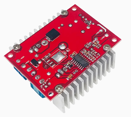
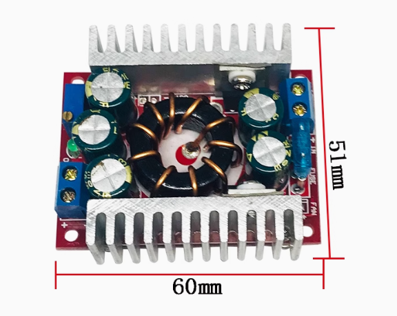
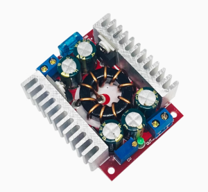
The 15A Adjustable DC-DC Synchronous Buck Converter is a high-power, high-efficiency step-down (buck) voltage regulator module designed for demanding applications in automotive, industrial, telecommunications, and embedded systems. Capable of delivering up to 15A of continuous output current with outstanding efficiency and low output ripple, this synchronous buck converter is an optimal solution for powering high-performance processors, FPGAs, DSPs, ASICs, and other power-hungry loads from higher voltage DC sources.
Synchronous buck converters are a type of DC-DC converter that uses both a high-side and a low-side MOSFET, replacing the traditional catch diode found in asynchronous designs. This synchronous rectification dramatically improves conversion efficiency, especially at low output voltages, reduces heat generation, and allows for higher output current capability in a smaller footprint.
This module accepts a wide input voltage range and provides an adjustable output voltage that can be set precisely to meet the requirements of your specific load. With advanced features such as cycle-by-cycle overcurrent protection, thermal shutdown, and soft-start, this module is engineered for reliability in professional environments .
Key Features
-
High Output Current: Capable of delivering up to 15A of continuous output current, suitable for powering high-performance processors, FPGAs, and industrial loads .
-
Synchronous Rectification Design: Utilizes both high-side and low-side MOSFETs (on-chip) to replace the traditional Schottky diode, achieving ultra-high efficiency and reducing heat dissipation .
-
Wide Input Voltage Range: Supports input voltages from 2.95V to 20V (package-specific), making it compatible with 3.3V, 5V, 12V, and 24V automotive and industrial power rails .
-
Adjustable Output Voltage: Output voltage is continuously adjustable down to 0.6V (or 0.5V on some models), enabling power delivery for low-voltage, high-current processors and logic circuits .
-
Low Output Ripple / Low Noise: Built-in high-gain bandwidth error amplifier and stable control loop provide excellent line and load transient response with minimal output noise .
-
High Reliability Protections: Comprehensive on-chip protection features including overcurrent protection (OCP), overvoltage protection (OVP), undervoltage lockout (UVLO), and thermal shutdown provide robust system-level reliability .
-
Wide Synchronization Range: Switching frequency can be synchronized to an external clock between 300 kHz and 1.5 MHz, allowing designers to avoid beat frequencies in sensitive multi-regulator systems .
-
Precision Voltage Regulation: ±1% internal voltage reference ensures accurate output voltage regulation under varying operating conditions .
-
Integrated Power MOSFETs: Ultra-low resistance power switches (as low as 4.3mΩ) are integrated directly into the controller, reducing external component count and simplifying design .
-
Thermally Enhanced Packaging: Advanced packaging (e.g., 20-pin HTSSOP, PowerPAK MLP34-57) with an exposed thermal pad for superior heat dissipation and industrial-grade reliability .
Technical Specifications
Pinout & Interface Guide
While specific pin configurations vary by chip manufacturer (TI, Vishay, Renesas, Analog Devices), the fundamental power and control pins for a synchronous buck converter are broadly similar.
Typical Pin Configuration
The following pins are typical for a high-current synchronous buck controller, such as the LM21215A or LTC7151S:
Power Pins
-
PVIN (Power Input): Connect to the main DC input voltage source (e.g., 12V automotive battery, 5V supply). Decouple with low-ESR ceramic capacitors placed close to the IC.
-
PGND (Power Ground): The high-current return path for the switching MOSFETs. Connect directly to the input and output capacitor grounds.
-
SW (Switch Node): The output of the internal power stage. Connect to the inductor here.
-
VOUT (Output Voltage): The regulated output voltage; connect to the load.
Control & Feedback Pins
-
FB (Feedback): The voltage sense pin for the feedback divider. The IC regulates the output by comparing this voltage to an internal reference (e.g., 0.6V or 0.5V).
-
COMP (Compensation): Internally or externally connected to the error amplifier output. Required for loop stability.
-
EN (Enable): Logic input to turn the regulator on/off. May have a precision threshold for undervoltage lockout.
-
PGOOD (Power Good): An open-drain output indicating the output voltage is within regulation.
-
SS/TRK (Soft-Start / Tracking): Capacitor or voltage set for soft-start and output tracking.
-
RT/SYNC (Resistor/Sync): Sets the switching frequency via a resistor or synchronizes to an external clock.
-
VCC: Output of the internal LDO for the gate drivers.
PCB Layout Considerations for 15A Design
-
High-Frequency Loop: The input capacitor, high-side MOSFET, low-side MOSFET, and power ground form the critical hot loop. This loop must be physically as small as possible to minimize EMI and switching noise.
-
Thermal Management: A 15A converter dissipates significant power. Use a PCB with thermal vias under the IC’s exposed pad to connect to an internal ground plane for heat sinking. Consider forced air cooling for continuous high-power operation.
-
Sensing: Use Kelvin sense connections for the feedback (FB) pin, connecting directly to the output capacitor’s positive terminal to avoid ground bounce noise.
-
Input Capacitors: Place high-quality ceramic input capacitors (multiple 10µF to 100µF) as close as possible to the IC’s PVIN and PGND pins to handle the high ripple current .
Usage Guide
Setting the Output Voltage
The output voltage is set by an external resistor divider:
VOUT = 0.6V × (1 + R1 / R2)
(The internal reference voltage is 0.6V on most 15A controllers) .
For a given desired output voltage, choose R2 ≤ 5kΩ to maintain noise immunity and then calculate R1, or vice versa.
Setting the Switching Frequency (For Fixed-Frequency Controllers)
The switching frequency is typically set by a resistor (R_FREQ) between the RT pin and AGND. Using a higher frequency (1.5MHz) reduces component size but increases switching losses. Use lower frequencies (300 kHz) for peak efficiency.
Soft-Start Capacitor
The soft-start capacitor (C_SS) controls the output ramp rate, limiting inrush current.
-
The time interval can be calculated as T_SS = C_SS × V_REF / I_SS (where I_SS is typically 5µA).
-
For a C_SS of 0.1µF, the soft-start interval is approx. 12ms.
Overcurrent Protection
These devices include cycle-by-cycle current limiting. The top MOSFET current is sensed each cycle. If the current exceeds the set limit, the PWM cycle is terminated to protect the IC and the load .
Frequent Applications
-
Point of Load (POL) Converters for FPGA, ASIC, and DSP Core Power.
-
Automotive Infotainment & ADAS Power Supplies.
-
Industrial Motor Drives and Control Logic.
-
Power over Ethernet (PoE) Devices.
-
High-Performance Computing (Servers, Storage, Telecom).
-
Battery Management Systems (BMS) and Power Tools.
-
LED Lighting Drivers (High-Power Applications).
-
Portable Electronic Devices requiring high-density power conversion.
Q: How much current can this synchronous buck converter actually deliver?
The module is rated for 15 Amps continuous. For short duration peaks (e.g., during processor load transients), you can slightly exceed this, but sustained loads over 15 Amps will require active cooling. The internal MOSFET switches are optimized for 15A operation .
Q: I heard that synchronous buck converters are more efficient than asynchronous ones. Is that true?
Yes, significantly. Asynchronous designs use a Schottky diode for the low-side switch. Synchronous designs replace this diode with a low-resistance MOSFET (4.3mΩ on the LM21215A), which drastically reduces conduction losses, especially at high output currents. This results in higher efficiency (up to 98%) and lower operating temperatures .
Q: What is the difference between a buck converter and a synchronous buck converter?
A standard (asynchronous) buck converter switches power through a MOSFET and a diode. A synchronous buck converter uses two MOSFETs—one for the high-side switch and one for the low-side switch. The low-side MOSFET provides a much lower resistance path for current than a Schottky diode, dramatically improving efficiency at high loads .
Q: Can I synchronize the switching frequency with an external clock to avoid interference in my RF system?
Yes. This family of 15A synchronous buck converters includes a dedicated pin (RT/SYNC) that allows you to drive an external TTL clock signal. The internal oscillator will phase-lock to this signal, allowing you to place the switching noise outside your sensitive frequency band .
Q: What output voltage options are available?
You can set the output voltage anywhere from 0.6V up to (VIN × max duty cycle) by using an external resistor voltage divider on the feedback (FB) pin . The lower limit is ideally suited for powering modern processors with very low core voltages.
Q: This is a very high-power 15A module. What are the main protections against faults?
The IC includes on-chip: Overcurrent Protection (OCP) (cycle-by-cycle), Overvoltage Protection (OVP), which will pull the output low if it exceeds a threshold; Undervoltage Lockout (UVLO) to prevent operation at low input voltages; and Thermal Shutdown (TSD) with hysteresis
Q: The module has adjustable switching frequency. Which frequency should I choose?
Design requires trade-offs:
-
High Frequency (1.5MHz): Smaller external components (inductor, capacitor), faster transient response, but higher switching losses.
-
Low Frequency (300kHz): Lower switching losses, better efficiency, but larger inductor and capacitor values required .
Q: What applications are 15A buck converters typically used for?
They are used to power high-performance loads such as FPGA and ASIC core rails, DSPs, servers, telecom equipment, industrial motor drive logic, automotive infotainment systems, and high-power LED arrays.
Q: Does this IC require a minimum load to regulate properly?
No. Many modern devices operate in Diode Emulation Mode (DEM) at light loads, which allows them to skip pulses and maintain high efficiency. They can operate with zero load current without losing regulation .
Q: What is the "Power Good" (PGOOD) pin used for?
The PGOOD pin is an open-drain output that goes high impedance (active high with external pull-up) when the output voltage is within regulation. This is commonly used for fault reporting and for sequencing the startup of other supplies (e.g., enabling a 1.8V rail only after a 3.3V rail is stable)