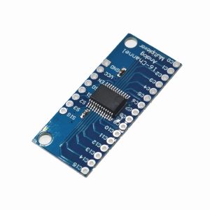


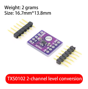

The TXS0102 2-Channel Bi-Directional Logic Level Shifter is a high-performance voltage translator designed specifically for modern digital interfaces. It provides a safe, seamless bridge for communication between components operating at different voltage rails, such as connecting a 1.8V sensor to a 3.3V microcontroller or a 3.3V controller to a 5V system.
Product Description
The TXS0102 is an advanced voltage-level translator that utilizes a specialized pass-gate architecture to enable true bidirectional communication without the need for a direction-control signal. This makes it exceptionally well-suited for open-drain applications like I2C (IIC) and SMBus, as well as push-pull applications.
Unlike simpler MOSFET-based shifters, the TXS0102 features integrated edge-rate accelerators that improve the rise times of signals, allowing for higher data rates across the voltage barrier. Its tiny footprint and high efficiency make it a favorite for both compact DIY wearable electronics and professional industrial PCB designs.
Features
- True Bidirectional Translation: No direction-control pin required; the device automatically senses and adapts to data flow.
- Optimized for I2C: Specifically designed to handle the pull-up requirements and timing of I2C/IIC and SMBus protocols.
- High Data Rates: Supports up to 24 Mbps in push-pull applications and 2 Mbps in open-drain setups.
- Edge-Rate Accelerators: Integrated circuitry improves signal integrity by sharpening digital transitions.
- Partial Power-Down Support: Features
IOFFcap I sub cap O cap F cap F end-sub
𝐼𝑂𝐹𝐹
circuitry that isolates the bus when the device is powered down, preventing backflow current.
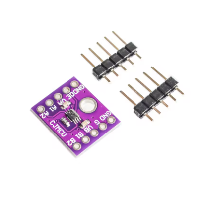
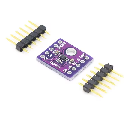
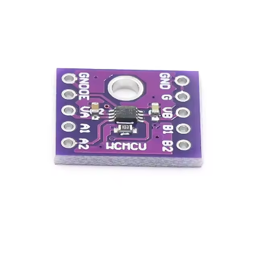
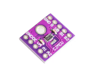
- Breadboard Friendly: Typically comes on a breakout board with standard 2.54mm (0.1″) pin spacing