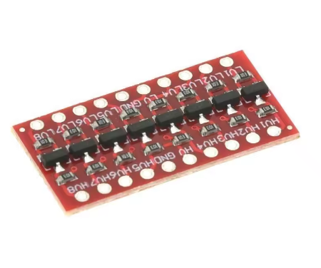


The 8-Channel Bi-Directional Logic Level Shifter (Red PCB Edition) is a robust and essential interface module designed for high-density digital communication. This board allows for safe, high-speed data transfer between devices operating on different logic voltages, such as connecting a 5V industrial controller to a 3.3V or 1.8V high-performance processor.
Product Description
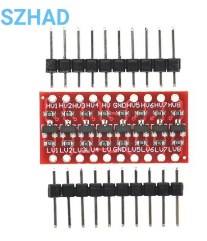
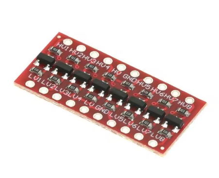
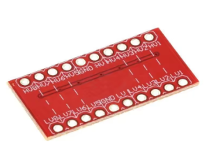
The 8-Channel Bi-Directional Level Shifter is a high-density voltage translator optimized for systems requiring multiple data lines, such as SPI, parallel interfaces, or complex sensor arrays. Built on a distinctive red PCB, this module utilizes high-speed N-channel MOSFETs with integrated pull-up resistors to provide 8 independent channels of bidirectional shifting.
Unlike smaller 2-channel or 4-channel modules, this 8-channel version is designed to handle entire data buses in a single, compact footprint. It effectively bridges the gap between different power domains (e.g., 5V, 3.3V, 2.8V, and 1.8V), protecting sensitive low-voltage microcontrollers like the Raspberry Pi or ESP32 from the higher voltages used by older legacy systems or 5V Arduino components. The bidirectional nature of the circuitry means it automatically adapts to data flowing in either direction, making it ideal for asynchronous communication and complex digital logic.
Key Features
- High Channel Density: 8 independent channels provide enough capacity for a full SPI bus plus additional control signals (like Reset or CS).
- True Bidirectional Capability: No direction-control signal is required; the hardware automatically senses the flow of data.
- Wide Voltage Range: Supports stepping between voltages as high as 5V and as low as 1.8V.
- Integrated Pull-Ups: Features onboard 10kΩ pull-up resistors on every channel to ensure clean signal transitions for I2C and GPIO.
- Safety Isolation: Prevents “back-powering” where a high-voltage pin accidentally powers a low-voltage rail through internal protection diodes.
- Prototyping Ready: Standard 2.54mm (0.1″) pin spacing for easy use with breadboards or standard ribbon cables